FINAL FINISHES
ENIG 
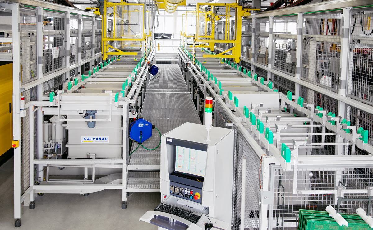
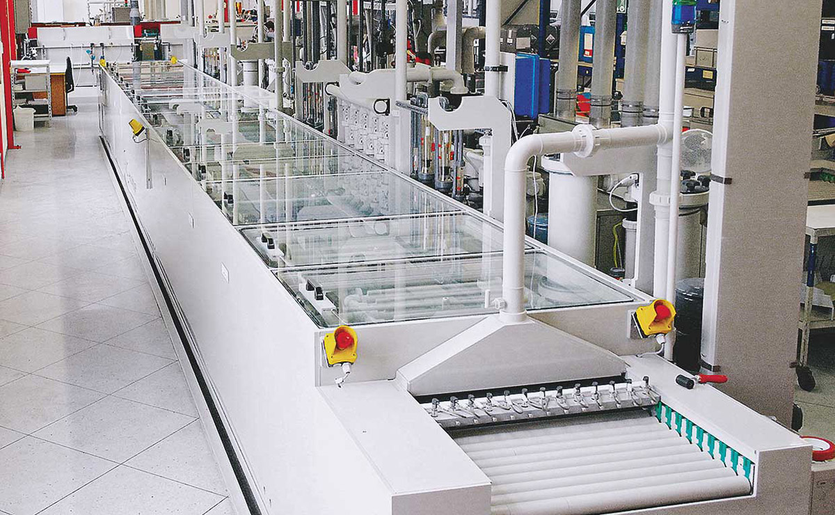
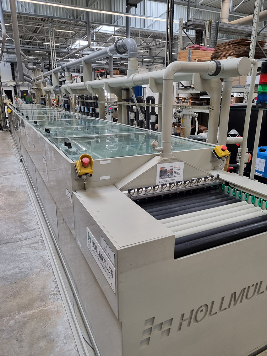
Modern system control and automatic dosing devices are prerequisites for a constant quality of the separation. We have various baskets available for a large number of format sizes and thicknesses. Non-destructiv corrosion control is an integral part of our quality control process.
| format | max. 700 x 605 mm min.100 x 200 mm |
 |
|
| plate thickness | 0.012 – 15 mm |
 |
|
| Aspect Ratio | 1:15 (Boreholes must be completely free developed and/or completely sealed) |
 |
|
| capacity | 1000 m² / day (ca. 2000 – 3000 Panel) |
 |
|
| phosphorus content Ni |
8 – 10 % |
 |
|
| hardness Ni | ca. 500 HV |
 |
|
| empf. Au layer thickness | 0.05 – 0.1 μm |
ENIG TRG 
Fully automatic basket systemElectroless nickel gold (ENIG) is known for its benefits:
Durability and longevity, excellent electrical conductivity, compatibility with a wide range of materials including lead-free soldering and excellent surface flatness.
Unfortunately, there are also disadvantages that need to be taken into account:
The deposition mechanism is based on a redox reaction in which gold is deposited from a gold salt solution while nickel is simultaneously dissolved from the surface to provide the electrons required for the reaction.
The challenge with ENIG plating is to minimise nickel corrosion in order to maintain the integrity of the nickel layer and at the same time ensure sufficient gold deposition of 0.05 – 0.1 µm.
ENIG TRG by Hofstetter solves this problem. A partially reducing gold electrolyte minimises nickel dissolution and significantly improves the quality of the gold layer. The nickel is not completely oxidised during the deposition process, i.e. practically no nickel is dissolved from the surface.
The layer system is characterised by the following properties:
- Low-corrosion deposition and excellent solderability
- Possibility of thicker gold deposition, which enables Au wire bonding
- Greater reliability and quality
| Gold layer TRG | Fine gold 99.9 % by weight |
 |
|
| Recommended layer thickness | 0.05 – 0.1 µm Soldering (Au wire bondability at < 0.2 µm; not suitable for Al wire) |
 |
|
| Nickel layer (mid phos) | 8 – 10% P, approx. 500 HV in as-plated condition |
 |
|
|
Plant engineering:
|
|
 |
|
| Vollautomatische Korbanlage | 500 m² / day |
 |
|
| Panel size |
max. 700 x 605 mm min. 100 x 200 mm |
 |
|
| Panel thickness |
0,012 – 15 mm |
 |
|
| Holes |
AR 1:15 (completely open or closed) |


ENEPIG 
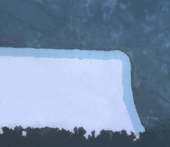
With the reductively deposited palladium as an intermediate layer, excellent bonding results are achieved with gold wire bonding. This layer is also very suitable for soldering applications and aluminum wire bonding. With the semi-reductiv gold process we use, nickel corrosion issues are a thing of the past. The ENEPIG by Hofstetter PCB surface therefore fulfils the highest quality requirements.
| format | max. 700 x 605 mm min. 100 x 200 mm |
 |
|
| plate thickness | 0.012 – 16 mm |
 |
|
| Aspect ratio drilling |
1:15 (Boreholes must be completely free developed and/or completely sealed) |
 |
|
| capacity | 500 m² / day |
 |
|
| Ni layer thickness* | 3 – 7 μm |
 |
|
| Pd layer thickness | 0,08 – 0,3 µm |
 |
|
| Au layer thickness | 0,03 – 0,08 µm |
EPIG 
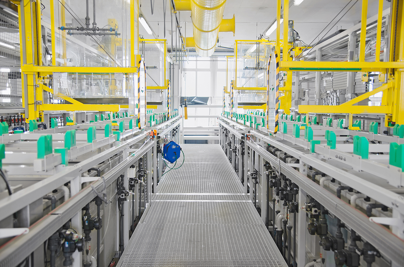
Electroless palladium gold is a nickel-free finish that can be used in a variety of ways. The layer is suitable for any type of soldering and bonding application. Palladium serves as a diffusion barrier and the gold layer thickness can be variably adjusted up to 0.3 µm thanks to the partially reductive character.
application
Reflow soldering and bonding (aluminum and gold wire) fine line, high-frequency and medical technology
layer properties
Planar surface, bondable with aluminum and gold wire as well as alternative bonding wires, storage time ≥ 12 months
layer thicknesses
0.1 – 0.2 µm Pd / 0.1 – 0.2 µm Auv
| format | max. 700 x 610 mm min. on request (ca. 100 x 100 mm) |
 |
|
| plate thickness | 0,012 – 10 mm |
 |
|
| Aspect ratio PTH |
1:16 (Boreholes must be completely free developed and/or completely sealed) |
 |
|
| Aspect ratio BV |
1:1 (after copper plating) |
 |
|
| capacity | 200 m² / day |
DIG 
The miniaturization of printed circuit boards as well as the increasingly demanding high frequency applications require new concepts for the surface finish. With the DIG-Process which is a semi-reductive gold deposition directly on copper, we now can offer a further alternative to the EPIG Process, as far as a multi-functional nickel-free final surface is concerned.
The final finish has excellent bending properties and is outstanding in the SAP sector in terms of the Fine-Line Technology. It has a very good solderability and also has excellent Au wire bonding properties. Despite the lack of a diffusion barrier, the final finish has already passed several tests and is already being used successfully in the medical and aviation sectors.
| format | max. 700 x 605 mm min. 100 x 200 mm |
 |
|
| plate thickness | 0.012 – 16.0 mm |
 |
|
| Aspect Ratio | 1:16 (Boreholes must be completely free developed and/or completely sealed) |
 |
|
| Aspect Ratio BV | 1:1 (after copper plating) |
 |
|
| capacity | 200 m² / day |
 |
|
| Au layer thickness* | 0.25 µm (0.2-0.3) |
* geringere Schichtdicken sind bei Lötanwendungen möglich, muss vom Bestücker geprüft werden
immersion Tin
The chemical tin process for lead-free multiple soldering and press-in technologies. In the electronics industry, immersion tin is recognized as a reliable surface for both printed circuit boards and IC substrates.
| format | max. 610 x 2000 mm min. 100 x 60 mm |
 |
|
| plate thickness | 0.012 – 5 mm |
 |
|
| Aspect Ratio |
1:16 (Boreholes must be completely free developed and/or completely sealed) |
 |
|
| Micro Vias |
1:1 |
 |
|
| layer thickness | 0.6 – 1.2 μm |
 |
|
| capacity | 1500 m² / day |
 |
|
| Reel to Teel |
on request |
immersion Silver
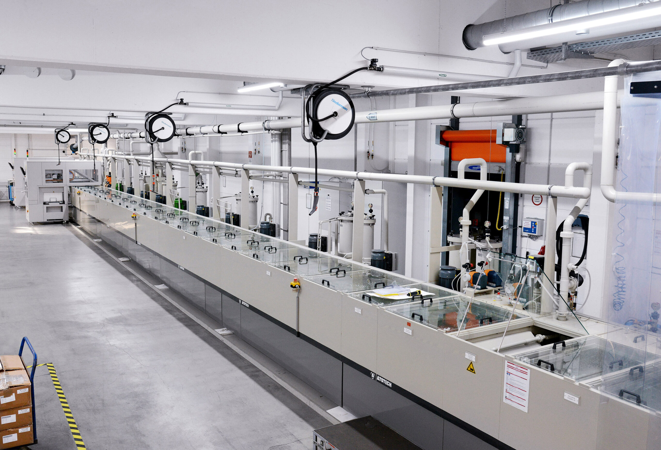
This lead-free surface shows very good soldering behavior even after aging. There is no growth of intermetallic phases during aging. The short process time results in good compatibility with a wide variety of solder resists
| format | max. 610 x 1500 mm min. 100 x 200 mm |
 |
|
| plate thickness | 0.05 – 6.0 mm |
 |
|
| Aspect Ratio |
1:12 (higher on request; boreholes must be completely free developed and/or completely sealed) |
 |
|
| Micro Vias | 1:1 |
 |
|
| layer thickness | 0.15 – 0.45 μm |
 |
|
| capacity | 1500 m² / day |
 |
|
| Reel to Reel | max. bandwidth 650 mm |
OSP
Glicoat-SMDF2(LX) coatings have excellent heat resistance and are compatible with non-clean soldering fluxers and solder pastes, making it ideal for use on SMD circuit boards and as an alternative to HAL and other finishes.
| format | max. 610 x 2000 mm min. 100 x 60 mm |
 |
|
| plate thickness | 0.012 – 5 mm |
 |
|
| Aspect Ratio |
1:16 (Boreholes must be completely free developed and/or completely sealed) |
 |
|
| Micro Vias |
1:1 |
 |
|
| layer thickness | 0.15 – 0.3 μm |
 |
|
| capacity | 500 m² / day |
 |
|
| Reel to Teel |
on request |
Electroplated nickel / gold
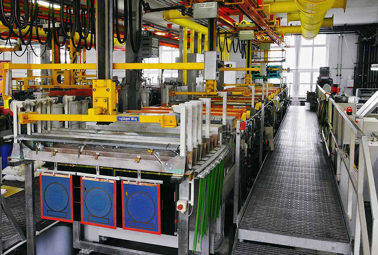
With the galvanic nickel/gold system, we can offer hard gold and bond gold coatings. Freely programmable sequences enable the construction of different layer combinations. We have flexible frame technology available for processing materials of different thicknesses.
| format | max. 610 x 900 mm min. 100 x 100 mm |
 |
|
| plate thickness | 0.050 – 20 mm |
 |
|
| MicroVias | 1:1 |
| layer properties: Electroplated nickel / gold |
|
| Nickel | hardness 400 – 450 HV |
 |
|
| hard gold | alloy cobalt purity 99,8% hardness 140 – 170 HV density 17 g/cm³ |
 |
|
| soft gold | purity 99.99% hardness 80 – 110 HV density 19.0 g/cm³ |
Reel to Reel
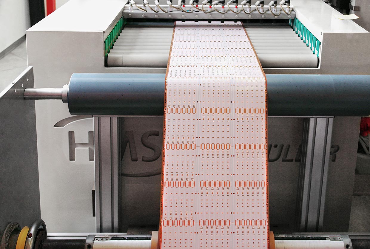
| bandwidth | max. 650 mm |
 |
|
| length | up to 300 m (depending on the material thickness) |
 |
|
| material | all common flex materials |
 |
|
| processes | OSP chemical tin chemical silver |
